
China’s Photonic Ascendancy: From Supply Chain Mastery to LightGen’s Breakthrough
How Beijing’s Strategic Investments in Silicon Photonics Birthed the World’s First All-Optical AI Chip and Reshaped the Future of Global Computing Power

Photonics promises transformative applications: lab-on-a-chip medical diagnostics, vehicle-to-infrastructure communication, environmental sensing (vibration, strain, CO2), and food quality analysis beyond human senses. By processing data with light—via waveguides, lasers, modulators, and detectors—PICs deliver higher bandwidth, lower heat, and greater miniaturization than electronic ICs, enabling ubiquitous connectivity with minimal energy loss.
China’s rapid advances in photonic technologies represent one of the most consequential shifts in the global technology landscape. My earlier Substack posts1 traced this trajectory: the building of a comprehensive domestic supply chain, the dawn of scalable photonic integrated circuits (PICs), the establishment of dedicated fabrication facilities, and the potential to permanently challenge American dominance in semiconductors. These developments, driven by state-led investment in indigenous innovation, reached a milestone last month with the unveiling of LightGen—an all-optical chip capable of running large-scale generative AI models with unprecedented speed and efficiency.
Foundation: Creating a Photonic Supply Chain
In China’s Photonic Supply Chain, below, I highlighted Beijing’s systematic construction of an end-to-end ecosystem for photonics, with heavy investments starting in 2003. Key nodes include Wuhan’s Optical Valley, a massive cluster with thousands of enterprises dominating global fiber optics and optoelectronics production.
Breakthroughs accelerated in 2024: CAS2 developed mass-producible silicon optical chips using lithium tantalate integration; Jiangsu South Huanghai Silicon (JSHS) achieved the first 12-inch optical-grade lithium niobate crystals with ambitions for 250,000 wafers annually; Peking University demonstrated a topological photonic chip with programmable optical lattices; and Tsinghua University introduced Taichi, an all-optical sensing and computing chip for edge applications like autonomous vehicles.
Shanghai Jiao Tong University (SJTU) launched a 17,000 sq.m. photonic pilot line producing 10,000 wafers yearly, covering full processes from lithography to packaging. Companies such as Amazec Photonics (medical sensors), PhotonFirst (structural monitoring), and MantiSpectra (chemical analysis via smartphones) illustrated practical applications in healthcare, infrastructure, and consumer tech. China’s global photonics market share surged from 10% to 32% while Western shares stagnated, thanks to a self-reliant chain avoiding high-end lithography dependencies. This ecosystem captures value across the board, positioning photonics as a strategic industry akin to batteries or EVs.
The Dawn of Practical Photonics: Scaling
Photonic Dawn framed these efforts as heralding America’s “electronic twilight.” Thin-
film lithium niobate (TFLN) emerged as a game-changer: SJTU produced the first 6-inch TFLN wafers, yielding 2.25 times more chips per wafer than 4-inch versions and slashing costs by 50%. Compatible with existing CMOS fabs like SMIC’s, TFLN overcomes lithium niobate’s manufacturing challenges while leveraging its superior electro-optic properties—up to 100 times better than silicon for modulation speed and efficiency. Mass production lines for multi-material photonic chips were slated for 2025 by firms like Sintone.
Ending American IC Dominance? Photonic Chips as the Disruptor
China’s Photonic Chips End America’s IC Dominance argued that PICs—using 10% of the power and running at 1000 times the speed of electronic equivalents—enable room-temperature quantum computing, scalable AI, and secure 6G communications.
SJTU’s CHIPX shipped the first TFLN photonic chips in 2024, achieving wafer-scale mass production and co-packaging of photons/electronics. With China controlling ~80% of TFLN wafer output and leading patents, these chips support hundreds of photonic qubits for drug discovery and entanglement-based encryption.
Energy advantages reduce data center cooling by 90%, while speed boosts enable ultrafast neural network inference. Geopolitically, this undercuts US controls, accelerates domestic AI/quantum ecosystems, and positions China to export via Belt and Road networks. The global photonics market, projected at $2 trillion by 2027, underscores the stakes.
Culmination: All-Optical Generative AI
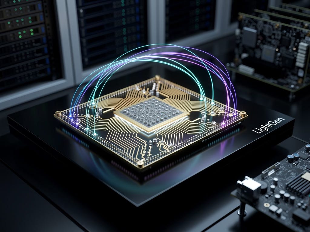
These foundational efforts crystallized in December 2025 with LightGen3, the world’s first all-optical chip for large-scale generative AI. It integrates 2 million photonic neurons on a compact 136 mm² (1/5 in².) die via densely stacked metasurfaces and 3D packaging.
Overcoming key bottlenecks—scale integration, dimensional transformation, and optical training—LightGen shows more than 100-fold (two orders of magnitude) gains in both speed and energy efficiency versus state-of-the-art electronic chips like NVIDIA’s A100 GPU. It will potentially run much higher with optimizations for light-speed network reconfiguration and Bayesian algorithms, enabling end-to-end optical loops without electronic intermediaries or heavy reliance on labeled data. It performs complex tasks like high-resolution (512×512) image synthesis, video manipulation, style transfer, denoising, 3D scene generation, and semantic editing effortlessly.
LightGen validates earlier predictions: photonics excels in generative workloads demanding massive parallelism, and its pure optical pathway eliminates conversion losses, addressing AI’s exploding energy demands – just when the US faces electricity restrictions.
A Post-Silicon Geopolitical Realignment
LightGen signifies China’s leap from supply chain builder to innovation leader in post-silicon computing. It accelerates sustainable AI, reduces reliance on power-hungry GPUs, and enables edge-deployable generative models for real-world applications.
Geopolitically, it amplifies the decoupling trend: photonics sidesteps lithography chokepoints, leverages China’s material dominance (e.g., lithium niobate4), and offers a path to AI sovereignty. While still lab-stage—facing challenges in input/output interfaces, system integration, and commercialization—the trajectory is clear. Combined with prior fabs and ecosystems, LightGen positions China at the forefront of the photonic era, potentially rebalancing global tech power for decades.
Photonics is a really, really big deal.
China's Photonic Supply Chain

From theoretical conception to incubation to pilot line, Beijing backs future industries driven by cutting-edge technologies IF they possess strategic, leading, disruptive, even indeterminate, characteristics. Their last choices – batteries, EVs, solar panels – succeeded because they correctly anticipated future needs. But creating such cutting-edge technologies at scale requires mobilizing entire industrial ecosystems and building out complete industry chains, with cluster companies as links to ensure capabilities in key materials and components and to capture the value added by each link
China's Photonic Dawn = America's Electronic Twilight

In Photonic Dawn last year’s post on this subject, we explored China’s efforts to fabricate photonic integrated circuits, ICs. Today it alone produces six-inch, thin-film lithium niobate photonic chip wafers, in affordable, commercial quantities. Best of all, they’re made in regular IC fabs, cost fifty-percent less and have 100% Chinese IP, thanks to researchers at Shanghai Jiao Tong University, SJTU.
World's First Photonic Chip Fab..

When the US banned China from participating in NASA projects, China built its own. When the US banned China from participating in the "international" space station, China built its own. When the US stopped China from participating in Europe's GPS project, China built its own. When the US blocked Israel's sale of AWACs to China, China built its own. When Trump imposed tariffs on Chinese products to reduce US the trade deficit, it went up. When Biden imposed sanctions on Xinjiang products, US imports from Xinjiang went up. When the US and its vassals imposed sanctions o kill Russia’s ruble, the ruble went up. When the US strove to maintain dollar hegemony by threats, sanctions, and attacks, more countries decoupled from the dollar. What do you think will be the result of the US banning the sale of semiconductor technologies to China? – Peter Man.
China's Photonic Chips End America's IC Dominance. Permanently?
Achieving co-packaging technology for photons and electronics, chip-level integration and wafer-scale mass production of photonic quantum chips – I believe this is a world first. SJTU Prof. Jin Xianmin.
The Chinese Academy of Sciences, CAS, is the world’s leading research institute.
Unveiled by Yitong Chen and colleagues from SJTU (with Tsinghua collaboration) in Science (DOI: 10.1126/science.adv7434).
Lithium niobate excels where photonics demands fast, efficient manipulation of light using electric fields, nonlinear processes, or acoustic waves. This makes it indispensable for converting electrical signals to optical ones, generating new frequencies, and processing light at high speeds with low power.