
Will China's New 1nm Chip Change How Chips Work?
Put memory and processing on an FeFET chip and get ultra-low power, in-memory computing. It scales to sub-1nm, aligns perfectly with next-gen AI needs.

This development is too important for a two-line summary in China’s Week, so here’s a brief heads-up on another IC breakthrough:
Memory and processing live together
China’s new 1-nanometer ferroelectric transistor from Peking University isn’t so much about squeezing transistors smaller to “catch up” with the West in chip-making lithography. Instead, it’s about changing the basic way future chips work—especially for AI—by making memory and processing live together in a smarter, more energy-saving design.
Think of a normal computer chip like a busy office: the “processor” (logic part) does calculations in one room, while “memory” (where data is stored) sits in a separate filing cabinet down the hall. Every time the processor needs information, it has to send someone running back and forth. That running back and forth uses a lot of electricity and creates delays—it’s the biggest bottleneck in today’s AI systems, which shuffle huge amounts of data constantly.
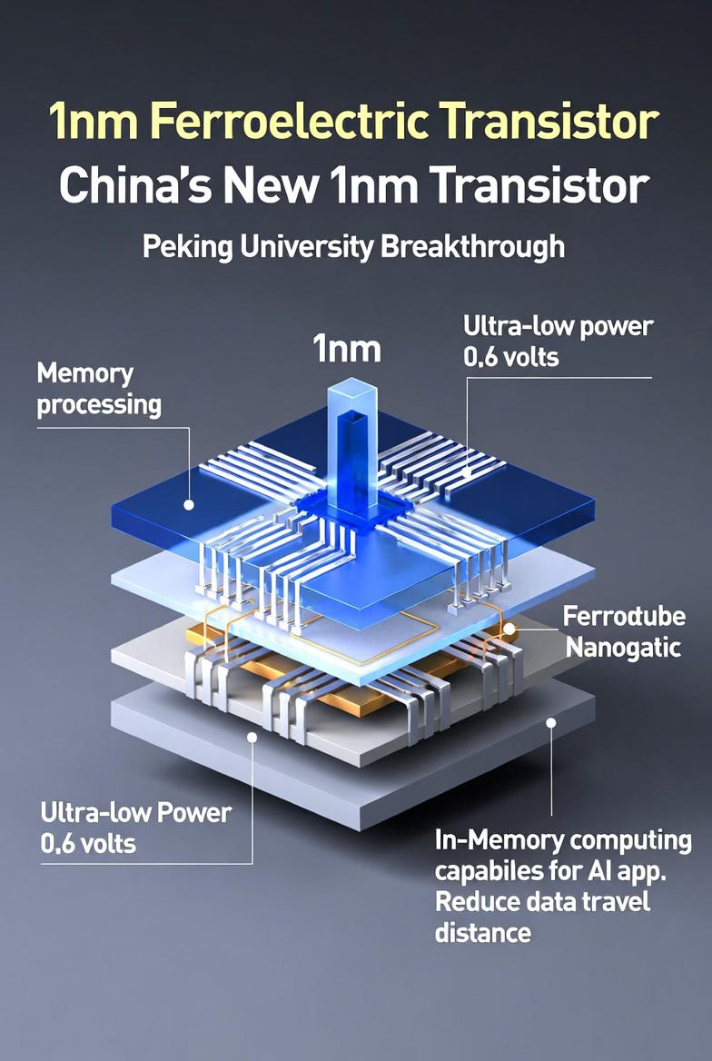
The Peking University team, led by Qiu Chenguang and Peng Lianmao, built a ferroelectric field-effect transistor (FeFET). Ferroelectric materials can “remember” their state (like a tiny magnet that holds its direction) even when power is off. This lets the transistor store data right inside itself, without needing a separate memory chip.
Nanogates
Their big innovation is a new ‘nanogate’: they used a super-tiny carbon
nanotube (1 nm wide) as the gate that switches the transistor on/off. This nanotube concentrates the electric field like a sharp needle, allowing the ferroelectric layer to flip its state at an ultra-low voltage of only 0.6 volts—much lower than previous FeFETs (1.5 volts) and now compatible with modern low-power logic circuits ( 0.7 volts or less).
Why this rewrites the architecture (not just shrinks things)
Ultra-low power: The device uses about one-tenth the energy of earlier ferroelectric designs and programs data in just 1.6 nanoseconds—super fast.
In-memory computing: Because memory and logic are fused in the same tiny unit, data doesn’t have to travel far. This could eliminate the “memory wall” that slows down AI, making chips that think more like the human brain (where processing and memory happen together in neurons).
Scales to sub-1nm: The design resists short-channel problems that usually wreck tiny transistors, opening the door to chips beyond today’s limits.
AI future: Researchers say this aligns perfectly with next-gen AI needs—efficient, brain-like hardware for edge devices, wearables, massive inference, and low-power data centers.
This lab breakthrough, published1 in Science Advances in February 2026, is still early-stage—no mass production yet—but it shows a different path: instead of racing on pure size (like 2nm or 1nm silicon processes), China is exploring new transistor types that could leapfrog traditional designs for energy-hungry AI. It’s less about matching TSMC’s node numbers and more about inventing a smarter transistor blueprint for tomorrow’s computers.
A very useful primer for people like myself who are ignorant of how progress is made in the development of semiconductors.